In 2024, new storage technologies such as DDR and HBM will shine!
2024-03-15 18:56:30
After the economic headwind of 2023 industry downcycle, the storage market will rise in 2024, and the price of memory chips will rise. In order to meet the demand of artificial intelligence heat wave in the past two years, the pace of innovation of new storage technologies has accelerated, and new technologies such as DDR, LPDDR and GDDR will usher in a volume cycle in 2024. HBM accelerated forward, HBM3/HBM3e continued to break through, is expected to drive the storage market to burst into new vitality.
one.
2024 is the year of DRAM technology bursting with vitality
From the earliest commercial DDR SDRAM chips produced by Samsung in 1998, to the continuation of DDR1, DDR2, DDR3, DDR4, and then to the mainstream DDR5 this year, and the upcoming DDR6 and DDR7, DRAM technology continues to break through. According to different application scenarios, the Solid State Technology Association (JEDEC) divides DRAM into standard DDR, LPDDR, GDDR three categories, of which DDR is mainly used in server and PC, LPDDR is mainly used in mobile phone and consumer electronics, the main application field of GDDR is image processing. Recently, the contribution of the above three types of DRAM technology new products to the original factory revenue continues to rise.
2024 is all about DDR5/LPDDR5
In the mainstream DRAM market pattern, Samsung, Micron, SK Hynix three parts of the world, the current DDR5/LPDDR5 market competition.
Take the above three as the mainstream. In addition, Taiwan storage companies Huabang and South Asia Technology, and mainland storage companies Changxin Storage are also positioned in the mainstream DRAM market.
From the past history, each generation of DDR new standards after the release of about 2 years of optimization, in order to achieve a more comprehensive and stable improvement in performance, and then to achieve the market replacement of the previous generation of products may take 3 to 5 years. Industry data shows that both DDR3 and DDR4 enjoy a life cycle of about seven years. The DDR4 memory standard was released in 2012, and its first generation entered the market in 2014 and did not achieve a significant increase in market share until 2016.
For the latest generation of DDR5, it has experienced a capacity climb and performance climb in the first half of 2023, and the proportion of revenue in the three original factories has been rising in the second half of the year, and officially ushered in the golden development period in 2024.
According to TrendForce consulting research shows that in the fourth quarter of 2023, Samsung's revenue reached 7.95 billion US dollars, a quarterly increase of more than 50%, mainly benefited from the 1alpha nm DDR5 shipment, making the Server DRAM shipments increased by more than 60%. SK hynix (SK hynix), although the shipments increased by only 1 to 3%, but continued to benefit from HBM, DDR5 price advantages, as well as profits from high-capacity Server DRAM modules, the average unit sales increased by 17 to 19%, the fourth quarter revenue reached $5.56 billion, an increase of 20.2%. Micron (Micron) volume and price, shipments and average unit sales are up 4 to 6% quarter, DDR5 and HBM proportion is relatively low, so the revenue growth rate is more moderate, the fourth quarter revenue reached $3.35 billion, an increase of 8.9% quarter.
In terms of LPDDR5, TrendForce Consulting believes that AI PC is expected to drive the average PC carrying capacity to increase, and increase the proportion of LPDDR in PC DRAM. In terms of Microsoft's definition of cpus that meet the NPU 40 TOPS, there are three and according to the shipment time, respectively, Qualcomm Snapdragon X Elite, AMD Strix Point and Intel Lunar Lake. Among them, the common denominator of the three cpus is that they all use LPDDR5x, rather than the current mainstream DDR SO-DIMM module, the main consideration is to improve the transmission speed; In terms of DDR5 specifications, the current speed is 4800-5600Mbps, while LPDDR5x is falling in 7500-8533Mbps, which will be helpful for AI PCS that need to accept more language instructions and shorten the reaction speed. Therefore, TrendForce Consulting expects that LPDDR will account for about 30-35% of PC DRAM demand this year, and will be supported by the specifications of AI PC CPU manufacturers in the future, thereby increasing the proportion of LPDDR imports.
Industry insiders say that due to the increasing maturity of DDR5/LPDDR5(X) technology, its shelf life may be longer than the previous generation. At present, storage manufacturers are focusing on HBM, DDR5 and LPDDR5(X) products.
TrendForce consulting research shows that in terms of capacity planning, Samsung significantly reduced production in the fourth quarter of last year, and after the improvement of inventory pressure, the first quarter of this year began to pick up, with a working rate of about 80%. In the peak season of the second half of the year, demand is expected to be significantly warmer than the first half of the year, and production capacity will continue to increase to the fourth quarter. SK Hynix actively expanded HBM production capacity, and the amount of film cast slowly increased, and with the HBM3e production, the relevant advanced process cast continued to rise. Micron has a temperature return trend, and will actively increase the proportion of 1beta nm in its advanced process for the production of HBM, DDR5 and LPDDR5(X) products, because of the increase in advanced process equipment, the production capacity will be more converging.
The GDDR7 video memory standard has been officially released
On March 6, the JEDEC (Solid State Technology Association) officially released the GDDR7 Graphics card (JES239 Graphics Double Data Rate (GDDR7)SGRAM) technical specification, designed to provide higher bandwidth, higher data transfer rates, higher energy efficiency and greater storage capacity to support the development of future high-performance computing applications.
The JESD239GDDR7 is the first JEDEC standard DRAM to use a pulse amplitude modulation (PAM) interface for high frequency operation. Its PAM3 interface improves the signal-to-noise ratio (SNR) for high-frequency operations while improving energy efficiency. By using 3 levels (+1, 0, -1) to transmit 3 bits in 2 cycles, compared to the traditional NRZ(non-return-to-zero) interface that transmits 2 bits in 2 cycles, PAM3 provides a higher data transfer rate per cycle, thereby improving performance.
Compared to GDDR6, GDDR7 has twice the bandwidth, up to 192 GB/s per device. This was achieved by increasing the number of independent channels to four. GDDR7 also supports densities from 16 Gbit to 32 Gbit and includes support for dual-channel modes that can double system capacity to meet the growing demand for high memory bandwidth for future graphics, gaming, computing, networking and artificial intelligence applications.
At the same time, the core-independent LFSR(Linear Feedback Shift Register) training mode, with blindfold and error counter, improves training accuracy while reducing training time. In addition, the RAS(Reliability, Availability, Maintainability) market needs are met by integrating the latest data integrity features, including on-chip ECC with real-time reporting (ODECC), data poisoning, error checking and cleaning, and command address parity with command blocking (CAPARBLK).
In terms of capacity, the current first batch of GDDR7 video memory is only 2GB(16Gb), which is consistent with today's GDDR6/6X, so the first NVIDIA RTX 50 series and AMD RX 8000 series have a larger demand for video cards. JEDEC said that there will be 3GB, 4GB, 6GB and even 8GB in the future, of which 3GB is the first time that this unconventional capacity has appeared.
Both AMD and NVIDIA have already joined the new standard, while Samsung and Micron have confirmed plans for the development of next-generation GDDR7 memory modules. Samsung is aiming for speeds of 32Gbps, while Micron is planning a 24Gb+ 32Gbps chip. It is reported that Micron has also announced in its latest roadmap to reach 36Gbps and 24Gb+ memory modules by 2026.
LPDDR6 memory specifications finalized in the third quarter of this year?
In addition, Korean media etnews recently quoted industry sources as saying that a new generation of mobile DRAM memory specifications LPDDR6 is expected to be announced in the third quarter of this year.
It is reported that the JEDEC Solid State Technology Association, an industry standard setting organization, recently held a consultation on the next generation of mobile random access processor standards in Lisbon, Portugal. During the meeting, the participants had a rich discussion and completed the final work of the LPDDR6 standard, which is expected to be officially released in the third quarter of this year.
Public information shows that the currently widely used LPDDR5 specification was released in 2019. The updated LPDDR5X specification was introduced in 2021 with several tweaks to achieve higher speeds, up to 8533Mbps. In addition, SK Hynix has also launched 9.6Gbps LPDDR5T products based on the private specification, and Micron has also launched LPDDR5X memory at the same rate.
In recent years, with its energy efficiency and speed advantages, the market for LPDDR has gradually expanded from traditional products such as smartphones to some server processors such as Nvidia Grace processors, as well as some AI-specific chips. With the wide application of AI, not only do mobile products require faster memory "feeding" end-to-side AI models than LPDDR5X, but the latter two types of processors also require greater memory bandwidth. At the same time, the three major uses have strict requirements for memory power consumption. Industry insiders said that the two main development priorities of the LPDDR6 standard are to improve data throughput and minimize power consumption.
According to etnews, Qualcomm Snapdragon 8 Gen 4 is expected to be the first product to support LPDDR6 memory.
two.
HBM technology is progressive and the market demand is huge
According to Wu Yating, senior vice president of research at TrendForce Consulting, the current 2024 HBM (High Bandwidth Memory) market mainstream is HBM3, and NVIDIA's new generation including B100 or H200 specifications are the latest HBM3e products. However, due to the high demand for AI, NVIDIA and other brands of GPU or ASIC supply is tight, in addition to CoWoS is the supply bottleneck, HBM is also the same, mainly because the HBM production cycle is longer than DDR5, the film to output and package completion takes more than two quarters.
Wu Yating said that at present, NVIDIA's existing memory solution for H100 is HBM3, and SK Hynix is the main supplier, but the supply is not enough to meet the needs of the overall AI market. By the end of 2023, Samsung will join the NVIDIA supply chain with 1Znm products, although the proportion is still small, but can be regarded as Samsung's primary gain in the HBM3 generation.
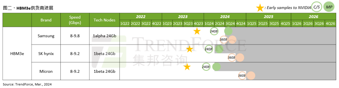
HBM3e is expected to volume quarter by quarter in the second half of the year, and Samsung and Micron have joined the supply ranks
Since Samsung is AMD's most important strategic supply partner for a long time, in the first quarter of 2024, Samsung HBM3 products have also passed the AMD MI300 series verification, including its 8h and 12h products, so since the first quarter of 2024, Samsung HBM3 products will gradually increase in volume. It is worth noting that in the past, in the product competition of the HBM3 generation, Micron has not joined the supply ranks, only two major Korean suppliers, and SK Hynix HBM market share is currently the highest, Samsung will follow the MI300 quarterly volume in the following quarters, and the market share will catch up.

Since 2024, the market focus has shifted from HBM3 to HBM3e, and it is expected that the volume will be increased quarter by quarter in the second half of the year, and gradually become the mainstream of the HBM market. According to TrendForce consulting survey, SK Hynix first passed the verification in the first quarter, followed by Micron, and began to submit HBM3e production products at the end of the first quarter to match the NVIDIA H200 planned to be rolled out at the end of the second quarter. Samsung, which submitted samples slightly later than the other two suppliers, expects its HBM3e to be validated by the end of the first quarter and begin shipping in the second quarter. Since the verification of Samsung HBM3 has made a breakthrough, and the verification of HBM3e is about to be completed if there is no accident, it also means that the company's shipment market share will close the gap with SK Hynix by the end of this year.
Sources say JEDEC is expected to relax the HBM4 standard, and hybrid bonding is still in the future
According to ZDNet Korea, industry standards-setting organization JEDEC Solid-State Technology Association is expected to relax the height restrictions on HBM4 memory, and memory manufacturers will not be forced to switch to Hybrid Bonding (Hybrid Bonding).
Key participants in JEDEC recently agreed to set the standard for HBM4 products at 775 microns (μm), thicker than the previous generation's 720 microns. It is reported that the agreement may have a significant impact on the future packaging investment trends of major memory manufacturers such as Samsung Electronics, SK Hynix and Micron.
The point of advanced packaging is to achieve greater interconnect density (more interconnects per region) and reduce trace length to reduce latency and energy per bit transmission. As a prominent presence in advanced packaging technology, hybrid bonding has been placed on high hopes since its birth.
Hybrid bonding is used for vertical (or 3D) stacking of chips. The salient feature of hybrid bonding is that it is convex free. It moves from solder-based bump technology to direct copper-to-copper connections. This means that the top die and bottom die are flush with each other. Neither chip has a bump, but only a brass pad that can be scaled to ultra-fine spacing. There is no solder, so solder-related problems are avoided. Hybrid bonding introduces a whole new set of technical and process challenges compared to previous bulk-based interconnects. In order to achieve high quality bonding, there are very strict requirements for surface smoothness, cleanliness and adhesion alignment accuracy.
The industry has said that "hybrid bonding will become the most transformative innovation in semiconductor manufacturing since EUV", whether the fact is we are not yet known, but we can see that Samsung Electronics, SK Hynix, Micron are chasing each other, competing to further break through this technology.
If JEDEC loosens the height restrictions on HBM4 memory, memory vendors need not rush to leap forward in bonding technology. With a package thickness of 775 micron, 16-layer DRAM stacked HBM4 can be fully realized using existing bonding techniques such as lead bonding, flip chip bonding, and through-silicon (TSV) bonding. After all, it is necessary to solve the problem of current market competition. And given the huge investment cost of hybrid bonding, memory companies are likely to focus on upgrading existing bonding technologies.
However, it is worth noting that the above mentioned bonding technology has its limitations and is not well suited to the increasing complexity and performance requirements of future 3D packaging. At present, the upstream and downstream of the semiconductor industry chain are full of expectations for the change of hybrid bonding technology, and with the increasing development of advanced process research and development, the market of hybrid bonding technology is worth looking forward to in the future.